|
By: Imran Ahmed, Copyright
2004-2008
1.1: Overview
1.2: Multiplying Digital to Analog
Converter (MDAC)
1.3: MDAC design considerations
(matching, thermal noise, switch sizes)
1.4: Opamp design - gain
requirement
1.5: Stage-ADC/Sub-ADC comparator
design
1.6: Summary
References
his tutorial discusses circuit implementations and related
design issues for 1.5 bit/stage pipeline ADCs. The key sub-blocks discussed
are: the stage MDAC, the stage ADC, and the stage amplifier.
As pipeline stages operate on discrete time signals (since
each stage has a sample and hold), switched capacitor circuits are used for
pipeline ADCs. With switch capacitor circuits it is possible to perform highly
accurate mathematical operations such as addition, subtraction, and
multiplication (by a constant), due to the availability of capacitors with a
high degree of relative matching. Switch capacitor circuits also facilitate
multiple, simultaneous signal manipulations with relatively simple
architectures. It is possible to combine the functions of sample and hold,
subtraction, DAC, and gain into a single switched capacitor circuit, referred
to as the Multiplying Digital-to-Analog Converter (MDAC) as shown in Fig.
1.
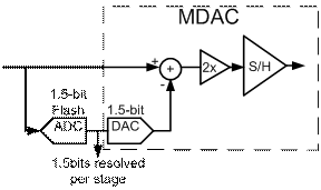
Fig. 1: MDAC functionality in dashes
Fig. 2 shows a single ended circuit implementation of the
MDAC of Fig. 1, using a switched capacitor approach.

Fig. 2: stage MDAC
The MDAC of Fig. 2 is shown single ended for simplicity,
although in practice fully differential circuitry is commonly used to suppress
common-mode noise [3]. A 1.5 bits/stage architecture has one of three digital
outputs, thus the DAC has three operating modes:
ADC output = 01: No over range error (stage input
is between –Vref/4 and Vref/4.
During  : QC1=C1Vin,
QC2=C2Vin : QC1=C1Vin,
QC2=C2Vin
During  : C1
is discharged, thus by charge conservation: C1Vin + C2Vin
= C2Vout (noting negative feedback forces node Vp
to a virtual ground). Thus : C1
is discharged, thus by charge conservation: C1Vin + C2Vin
= C2Vout (noting negative feedback forces node Vp
to a virtual ground). Thus
 è if C1=C2, then: Vout=2Vin (0.1) è if C1=C2, then: Vout=2Vin (0.1)
ADC output = 10: Over range error – Input exceeds
Vref/4, thus subtract Vref/2 from input
During : QC1=C1Vin,
QC2=C2Vin
During : C1 is
charged to Vref, thus by charge conservation
C1Vin
+ C2Vin = C1Vref +C2Vout
 è if C1=C2, then: Vout=2Vin-Vref
=2(Vin-Vref/2) (0.2) è if C1=C2, then: Vout=2Vin-Vref
=2(Vin-Vref/2) (0.2)
ADC output = 00: Under range error – Input below
-Vref/4, thus add Vref/2 to input
During : QC1=C1Vin,
QC2=C2Vin
During : C1 is
charged to -Vref, thus by charge conservation
C1Vin
+ C2Vin = C1(-Vref )+C2Vout
 è if C1=C2, then: Vout=2Vin+Vref
=2(Vin+Vref/2) (0.3) è if C1=C2, then: Vout=2Vin+Vref
=2(Vin+Vref/2) (0.3)
Thus the switched capacitor circuit implements the stage
sample-and-hold, stage gain, DAC, and subtraction blocks.
Signal dependent charge injection is minimized by using
bottom plate sampling, where the use of an advanced clock  , makes
charge injection signal independent [4]. A non-overlapping clock generator is
thus required for the MDAC. , makes
charge injection signal independent [4]. A non-overlapping clock generator is
thus required for the MDAC.
From equations (3.1)-(3.3) it is clear stage gain is
determined by the ratio of capacitors C1 and C2. Thus to
ensure a gain which is at least 10-bit accurate, C1 and C2
must match to at least 10-bit accuracy or within 0.1% for the first stage in
the pipeline. To obtain at least 0.1% matching a high quality capacitor such
as a Metal-Insulator-Metal (MIM) capacitor must be used. If properly
designed in layout, MIM capacitors can achieve matching between 0.01-0.1% [5].
MIM capacitors however are often unavailable in purely digital processes,
necessitating alternative capacitor structures. Alternatively metal-finger
capacitors, which derive their capacitance from the combination of area and
fringe capacitance between overlapping metal layers can be used in digital
processes to achieve sub 0.1% matching. Metal-finger capacitors however can
have large absolute variation (>20%), thus require a conservative design
approach. Alternatively a digital calibration algorithm can be employed to
significantly minimize mismatch-induced gain errors (and finite opamp gain
errors) [6], [7], [8], [9]. Due to additional design complexity, calibration
schemes are beyond the focus of this dissertation. We note however that
calibration techniques are emerging as essential approaches for high-resolution
pipeline ADCs due to the relaxed accuracy constraints afforded.
In addition to capacitor matching, it is essential the
ratio of capacitors C1 and C2 be linear for the desired
input range to minimize harmonic distortion. Thus non-linear parasitic gate
capacitance (MOS-caps), or other active capacitors should be avoided for C1
and C2 in high precision pipeline ADCs. Passive MIM, and
metal-finger capacitors are linear well beyond the 10-bit level, thus are
typically used.
The MDAC shown in Fig. 2 is a popular MDAC architecture,
as the capacitor sizes of C1 and C2 are equal. Since C1=C2,
identical layouts can be used for C1 and C2 - maximizing
layout symmetry and hence maximizing accuracy. As MIM capacitors only have a
marginal matching for 10-bit accuracy, a high degree of capacitor matching is
essential to minimize INL/DNL errors. Another advantage of the architecture of
Fig. 2 is a high beta value (feedback factor), which maximizes the bandwidth of
the closed loop system [10].
Although capacitors are ideally noiseless elements, in a
sampled system, sample and hold capacitors capture noise generated by noisy
elements such as switch resistors, opamps, etc. Consider the following noise
analysis of a capacitor sampling resistor noise as shown in Fig. 3:
Fig. 3: RC noise model
from [1] it is shown equivalent
noise bandwidth is  , ,
 [1] [1]
 è è  (0.4) (0.4)
From the above example it is clear increasing the size of
the sampling capacitor reduces the power of thermal noise. As thermal noise
represents a dynamic noise source that reduces ADC SNR, a minimum capacitance
(i.e. C1, C2) must be driven to ensure a sufficient
accuracy – thus thermal noise imposes a tradeoff between power and accuracy.
For the MDAC of Fig. 2, the effective input referred thermal noise, which
includes switch, and opamp noise is derived in [11] and found to be
 (0.5) (0.5)
where is the equivalent
output load capacitance, and Copamp the input capacitance to the
opamp. The relationship between SNR and minimum capacitor size for a full
scale signal swing of 0.8V, and C1=C2=Copamp=0.5pF
is shown in Fig. 4. is the equivalent
output load capacitance, and Copamp the input capacitance to the
opamp. The relationship between SNR and minimum capacitor size for a full
scale signal swing of 0.8V, and C1=C2=Copamp=0.5pF
is shown in Fig. 4.
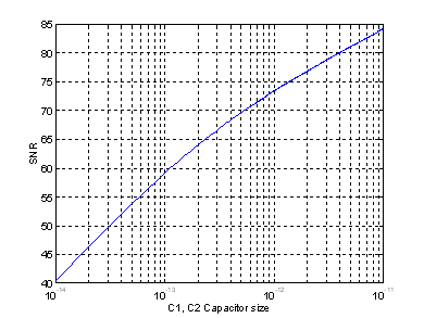
Fig. 4: Variation of SNR due to thermal noise (ignoring quantization error, full
scale=0.8V, C1=C2=Copamp=0.5pF)
From Fig. 4 it is clear thermal noise can alone limit
accuracy to less than 10-bits (SNR=62dB) if capacitors are not sufficiently
sized. As thermal noise represents only one of several precision limiting
factors (others include: quantization noise, power supply noise, capacitor
mismatch, etc.), it is desirable to place the noise floor beyond the 10-bit
level (e.g.) for thermal noise less than 1/4 LSB è
thermal noise floor should be at least -72dB. The stage accuracy requirements
are relaxed for subsequent pipeline stages. Thus it is possible to increase
the noise floor for subsequent stages by using smaller capacitors - maximizing
opamp bandwidth and minimizing overall power.
When sizing a MOS switch two key issues should be
considered: 1.) The desired RC time constant, and 2.) The maximum distortion
tolerable through the switch.
As switched-capacitor circuits have a finite time to
settle, it is essential the switches be sized large enough such that the
sampled signal settle to the desired accuracy in the allotted time. Since  ,
switch resistance can be minimized by increasing the MOS switch W/L ratio.
However an increased W/L ratio implies a larger area, which imparts a larger
parasitic capacitance to the circuit. As described in [1], a sufficiently
large parasitic capacitance can alter charge-sharing equations, and introduce
harmonic distortion through charge injection. Thus switch transistors must be
carefully sized, where switches should be large enough to ensure a sufficient
RC time constant, but small enough to minimize parasitic induced errors. ,
switch resistance can be minimized by increasing the MOS switch W/L ratio.
However an increased W/L ratio implies a larger area, which imparts a larger
parasitic capacitance to the circuit. As described in [1], a sufficiently
large parasitic capacitance can alter charge-sharing equations, and introduce
harmonic distortion through charge injection. Thus switch transistors must be
carefully sized, where switches should be large enough to ensure a sufficient
RC time constant, but small enough to minimize parasitic induced errors.
A consequence of the switch’s resistance dependency on Veff
is an RC time constant that is signal dependent, hence non-linear. A
non-linear RC time constant can lead to significant distortion if the switch
passes a continuous time signal, as is the case in front-end sample and hold
inputs. Signal–dependent RC time constants also affect discrete time signals,
as the MOS switch must be sized sufficiently such that the worst-case RC time
constant (i.e. when Veff is smallest) is sufficient for the desired
sampling speed. Non-linear RC time constants can be significantly minimized
however using a bootstrapping approach [4], which maintains a constant and
maximal Veff, thereby minimizing signal dependent variations.
The charge transfer relations derived in equations
(3.1)–(3.3) were based on the assumption of a perfect virtual ground at node Vp
in Fig. 2, which only occurs when the opamp gain is infinite. In practice
opamp gain is finite - introducing an error into the charge balance equations.
As such opamp gain must be made sufficiently large to minimize finite gain
error.
Consider the closed loop gain of a negative feedback
system H(s), as shown in Fig. 5:
 (0.6)
(0.6)
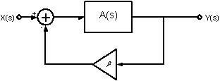
Fig. 5: basic linear feedback structure
Ideally as A(s) tends to infinity, H(s) è 1/b.
Thus the relative error ( ) is ) is
 (0.7) (0.7)
As switch capacitor circuits settle to DC values, DC gain
affects charge transfer equations:
 (0.8) (0.8)
Hence for an error due to finite opamp gain to be less
than ¼ LSB, i.e. 1/(4x1024)=1/(4096), with b=0.5
implies A > 8192, or A >78dB. Fig. 6 illustrates the variation of
relative error with opamp gain.
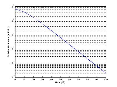
Fig. 6: gain error variation with opamp gain
Attaining 78dB of DC gain while maintaining a reasonable
bandwidth is near impossible with a simple single stage configuration (e.g.
differential pair) for sub-micron technologies. Thus two-stage or gain-boosted
configurations are necessitated for 10-bit pipeline ADCs (a detailed
description of high gain opamps is given in [1], [12]). It is noted that stage
accuracy requirements decrease along the pipeline, thus latter stages may have
less gain, allowing for simpler opamps (single stage, or no gain-boosting),
thus reducing power.
It should be noted that alternative MDAC architectures
exist which employ gain-error cancellation methods, facilitating much lower
opamp gains [6], [7], [8], [9] than those required by (3.8). Such approaches
however introduce a design overhead, and increase design time, thus are not
considered in this dissertation.
Switched capacitor circuits have a finite time in which to
settle, thus to ensure a minimum settling accuracy, opamp bandwidth must be
optimized. If the opamp is modeled as a first order system, the opamp transfer
function near the unity gain frequency is given by: [1].
Thus the MDAC step response, during is given by [1].
Thus the MDAC step response, during is given by
 (0.9) (0.9)

where  , and slew rate is
ignored. Since , and slew rate is
ignored. Since , where x is the
settling accuracy in bits, the available time to settle is , where x is the
settling accuracy in bits, the available time to settle is
 (0.10) (0.10)
As the available time t to settle is half the clock
period, 
 ,
(0.11) ,
(0.11)
 (0.12) (0.12)
where for settling within ¼ LSB,  for a 10-bit
ADC. Figure Fig. 7 graphically illustrates the required opamp unity gain
bandwidth to achieve a desired sampling rate and settling accuracy. for a 10-bit
ADC. Figure Fig. 7 graphically illustrates the required opamp unity gain
bandwidth to achieve a desired sampling rate and settling accuracy.

Fig. 7: required opamp unity gain frequency versus sampling frequency and settling
accuracy
From Fig. 7 and equations (3.11)-(3.12), a unity gain
frequency much larger than sampling frequency is required to obtain high
accuracy settling. Since the MDAC opamps must drive large capacitive loads (to
minimize thermal noise), much power is consumed by the opamps. As such, the
power consumption of opamps in a pipeline ADC often consumes 60-80% of the
total ADC power. However, the accuracy requirements decrease along the
pipeline, thus the unity gain frequency of subsequent stages along the pipeline
can be reduced, minimizing total power [2].
A flash architecture is commonly used for the stage ADCs,
due to low accuracy required by the stage ADCs. Flash ADCs consist of
comparators at the various thresholds of the ADC. For a 1.5-bit/stage pipeline
architecture stage flash ADCs require comparators at thresholds of +/-Vref/4
and 0. Digital error correction could be used to relax the tolerable offset on
stage-ADC comparators (up to +/-Vref/4). For Vref=0.8V, the comparator offset
can be as high as 200mV, which allows for minimum size devices in the
comparator (hence minimizing parasitic capacitance, thus minimizing power).
The relaxed offset constrains also afford simpler dynamic comparator
architectures, which do not require pre-amp gain stages, or static comparators
(e.g.: as used in. 6-bit flash ADCs [13], [14]). Like digital logic, dynamic
comparators only consume power on clock edges according to fCV2
thus have a power that scales linearly with sampling frequency. For pipeline
ADCs one of two dynamic comparators are typically used [15]: the Lewis and Gray
comparator [16] (Fig. 8), or the charge-distribution comparator (Fig. 9).

Fig. 8: Lewis and Grey comparator

Fig. 9: switched capacitor/charge distribution comparator
The Lewis and Gray comparator compares two fully
differential signals  , and , and  (Fully
differential comparators are highly desirable to reduce common-mode noise which
can be large in digital environments). Comparators at Vref/4 and –Vref/4 are
required to implement the 1.5bit/stage architecture, and comparators at Vref/2,
and –Vref/2 for the 2-bit flash at the end of the pipeline. Rather than supply
multiple reference voltages for each unique threshold, it is possible using the
architecture of Fig. 8 to derive an arbitrary threshold by appropriate device
sizing. Transistors M1-M4 operate in triode while the remaining transistors
implement positive feedback to resolve the differential input [11]. The
equivalent triode conductance of M1 and M2 from Fig. 8 are: (Fully
differential comparators are highly desirable to reduce common-mode noise which
can be large in digital environments). Comparators at Vref/4 and –Vref/4 are
required to implement the 1.5bit/stage architecture, and comparators at Vref/2,
and –Vref/2 for the 2-bit flash at the end of the pipeline. Rather than supply
multiple reference voltages for each unique threshold, it is possible using the
architecture of Fig. 8 to derive an arbitrary threshold by appropriate device
sizing. Transistors M1-M4 operate in triode while the remaining transistors
implement positive feedback to resolve the differential input [11]. The
equivalent triode conductance of M1 and M2 from Fig. 8 are:
 (0.13) (0.13)
 (0.14) (0.14)
The comparator threshold occurs when the circuit is
perfectly symmetric, i.e. when G1=G2, thus if W1=W4,
and W2=W3
 (0.15) (0.15)
where Vin = Vin+ - Vin-,
and Vref = Vref+ - Vref-
Thus it is possible to achieve thresholds at ±Vref/4, and ±Vref/2 by providing a common differential
reference voltage to each comparator in the pipeline, but sizing each
comparator to yield the desired threshold (e.g.: W2 = 4W1
for a threshold of Vref/4, W2 = 2W1 for a threshold of
Vref/2, etc.). As the comparator is fully differential, thresholds at –Vref/4
and –Vref/2 can be realized by reversing the polarity to the reference
voltage. Thus all required thresholds for a 1.5 bit/stage pipeline can be
realized by only supplying only one fully differential reference potential to
the chip.
A drawback of the Lewis and Gray comparator is the
threshold is a significant function of device symmetry. As the value resolved
by the comparator operates by comparing the integral of the ratio of current to
node capacitance at nodes V1 and V2, circuit symmetry is
crucial to reduce offset. Thus the layout of the Lewis and Gray comparator
requires great care, and parasitic extraction for full characterization of
input-referred offset. In [15] the Lewis and Gray comparator is shown to have
an offset of >200mV for a 0.35mm
CMOS process,
Alternatively a charge distribution approach can be used
to achieve a lower offset at the cost of increased power. As shown in Fig. 9,
the charge distribution approach uses charge conservation to derive a comparator
threshold, which depends on the ratio of capacitors rather than the ratio of
device widths and parasitic capacitances. Using a two-phase clock (,),
capacitors Cin and Cref are charged to and
respectively (in a
differential sense) on the first clock phase. The charge is forced to
redistribute between both capacitors during the second clock phase, where
according to charge conservation the effective threshold of the comparator is
found to be [15]
 (0.16) (0.16)
As the threshold is primarily a function of passive
components and largely independent of parasitic capacitance, a lower offset can
be achieved using the charge-distribution comparator. An analysis in [15]
compares fabricated implementations (in 0.35mm
CMOS) of the Lewis and Gray, and charge distribution comparators, where the
following silicon measured results were obtained:
Table 0‑1: Comparison of comparator area, offset, and power
|
Comparator
|
Area
|
Power
@ 100Msps
|
Voffset-max
|
|
Lewis
and Grey
|
1200mm
|
0.32mW
|
290mV
|
|
Charge
distribution
|
2800mm
|
0.81mW
|
75mV
|
As other offsets besides device mismatch (e.g. noise)
affect the stage transfer function, it is desirable to keep comparator offsets
below Vref/4. It should be noted the reduced offset of the charge distribution
comparator comes at the cost of increased power (due to the dynamic charging of
the sampling capacitors, and switches) and area. Thus the choice of which
comparator architecture to use requires a tradeoff between tolerable offset,
desired power consumption and area.
In this chapter circuit level implementation and design
related issued were discussed for key components in a 1.5 bit/stage pipeline
ADC: the stage MDAC and stage ADC comparators. It was shown for a desired
settling accuracy, MDAC opamps require a minimum gain and unity gain
bandwidth. Noise limitations due to thermal and opamp noise were shown limit
minimum MDAC sampling and feedback capacitor sizes. Two popular dynamic
comparators were examined: the Lewis and Gray comparator, and the charge
distribution comparator, where it was shown the optimal comparator was a
tradeoff between power and input referred offset.
. References
[1]
Johns, David and Martin, Ken. Analog Integrated Circuit Design.
John Wiley & Sons, Inc: New York, 1997.
[2]
P.T.F. Kwok et al, “Power Optimization for Pipeline Analog-to-Digital
Converters”, IEEE Transactions on Circuits and Systems--II: Analog and
Digital Signal Processing, vol 36, May 1999, pp. 549-553
[3]
Y. Park et al, “A low power 10 bit, 80MS/s CMOS pipelined ADC at 1.8V
power supply”, 2001 IEEEE International Symposium on Circuits and Systems
(ISCAS), vol 1, pp. 580-583
[4]
A. Abo, “Design for Reliability of Low-voltage, Switched-capacitor
Circuits”, Doctor of Philosophy in Electrical Engineering, University of California Berkeley, 1999
[5]
C. Diaz et al, “CMOS Technology for MS/RF SoC”, IEEE Transactions on
Electron Devices, vol 50, March 2003, pp. 557-566
[6]
J. Li et al, “Background Calibration Techniques for Multistage Pipelined
ADCs With Digital Redundancy”, IEEE Transactions on Circuits and Systems –
II: Analog and Digital Signal Processing, vol 50, September 2003, pp.
531-538
[7]
Y. Chiu et al, “Least Mean Square Adaptive Digital Background
Calibration of Pipelined Analog-to-Digital Converters”, IEEE Transactions on
Circuits and Systems – I: Regular Papers, vol 51, Janurary 2004, pp. 38-46
[8]
S. Chuang et al, “A Digitally Self-Calibrating 14-bit 10-MHz CMOS
Pipelined A/D Converter”, IEEE Journal of Solid-State Circuits, vol 37,
June 2002, pp. 674-683
[9]
B. Murmann et al, “A 12-bit 75-MS/s Pipelined ADC Using Open-Loop
Residue Amplification”, IEEE Journal of Solid-State Circuits, vol 38,
December 2003, pp. 2040-2050
[10]
W. Yang et al, “A 3-V 340-mW 14-b 75 Msample/s CMOS ADC with 85dB SFDR
at Nyquist Input”, IEEE Journal of Solid State Circuits, Brief Paper,
vol 36, December 2001, pp. 1931-1936
[11]
T. Cho, “Low power Low voltage A/D conversion techniques using pipelined
architecture”, Doctor of Philosophy in Engineering, University of California Berkeley, 1995
[12]
Razavi, Behzad. Design of Analog CMOS Integrated Circuits. McGraw-Hill, New York, 2000
[13]
Uyttenhove et al, “A 1.8-V 6-bit 1.3-GHz flash ADC in 0.25mm CMOS”, IEEE Journal of Solid-State
Circuits, vol 28, July 2003, pp. 1115-1122
[14]
M. Choi et al, “A 6-b 1.3-Gsample/s A/D converter in 0.35-mm CMOS”, IEEE Journal of Solid-State
Circuits, vol 36, December 2001, pp. 1847-1858
[15]
L. Sumanen et al, “CMOS dynamic comparators for pipeline A/D
converters”, 2002 IEEE International Symposium on Circuits and Systems
(ISCAS), vol 5, 2002, pp. 157-160
[16]
L. Sumanen et al, “A mismatch insensitive CMOS dynamic comparator for
pipeline A/D converters”, 2000 International Conference on Electronics,
Circuits and Systems (ICECS), pp. 32-35
|
