|
ADC Architectures Tutorial
Imran Ahmed,
Copyright 2004-2008
1.1: Overview
1.2: Analog vs. Digital
Information
1.3: Flash ADC archtiecture
1.4: Speed, Power, Accuracy
tradeoffs in ADCs
1.5: Alternative ADC architectures
1.6: Pipelined ADC architecture
1.7: Error correction in Pipelined
ADCs explained with long division
1.8: Summary
References
n this tutorial a comparison of analog versus digital
information is given, where the superior noise resilience of digital signals is
shown to necessitate digital signaling for modern high-speed signaling
environments. Non-idealities that are analog in nature are shown to
necessitate ADCs in the digital signal path, which allow for signal recovery in
the digital domain. A brief discussion of the Flash ADC is given, followed by
a detailed analysis of the system level design of a 1.5 bit/stage pipeline
ADC.
Analog signals have an infinite number of output states,
whereas digital outputs have a finite number of states. Illustrations of
analog and digital signals are given in Fig. 1‑1, and Fig. 1‑2
respectively.
|

Fig. 1‑1: Example of an analog signal
|

Fig. 1‑2: Example of a digital binary signal
|
As digital signals have a finite symbol set, they are much
easier to accurately recover at a receiver than analog signals. For example if
a transmitted binary digital signal is distorted by a white noise source, it is
still possible to precisely determine if a ‘1’ or ‘0’ was transmitted so long
as the noise source is sufficiently small (maximum noise limitations on digital
signaling can be found in [1]). If a transmitted analog signal encounters the
same noise source however, the received analog signal is permanently distorted
as shown in Fig. 1‑3, thus the transmitted signal cannot be accurately
recovered (since an analog signal can be any value between maxima, the receiver
cannot accurately distinguish the noise from the signal). With modern
communication systems requiring fast and accurate signaling over noisy channels
(E.g.: air, telephone wires, coaxial cables, power lines, etc.), digital
transmission as shown in Fig. 1‑4 is commonly used.
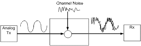
Fig. 1‑3: Analog signal transmission
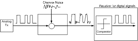
Fig. 1‑4: Digital signal transmission of binary data
Although digital transmissions facilitate simpler
receivers, channel distortion (e.g. echo, cross-talk, skin effect losses,
etc.), which cannot be removed with a single comparison operation as shown in Fig.
1‑4, necessitate more complicated receivers which perform a mathematical
analysis to recover the transmitted signal. As a mathematical analysis can be
easily performed in the digital domain, an ADC is required to convert the noisy
receiver input to a digital representation for digital signal processing, as
shown in Fig. 1‑5.
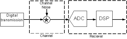
Fig. 1‑5: ADC in signal path of a digital communication system
In general ADCs are required blocks when a digital system
interfaces with an analog environment.
Various ADC architectures have been developed over the
years, each with different tradeoffs with respect to power, speed, and accuracy
(details in section 1.5). Most ADC architectures however are in some form a
variant of the Flash ADC. Flash ADCs operate much like a ruler: a ruler with a
fixed resolution (e.g. can measure accurately to millimeters) measures an
infinite precision length to a finite accuracy. Flash ADCs measure an
analog signal into a digital signal by comparing an analog input to fixed
reference values as shown in Fig. 1‑6. The number of fixed references
used determines the accuracy of the digital output (e.g.) 4-bit accuracy is
obtained by comparing against 24=16 reference values, 10-bit
accuracy by comparing against 210=1024 reference values.
Determining which reference values the input is in-between forms a length 2N
bit (where N is the accuracy of the ADC) thermometer code representation of the
analog input. Mapping the unique thermometer code to its binary equivalent
forms a length N, binary representation of the analog input [2].

Fig. 1‑6 Analogy between ruler and Flash ADC
Note from Fig. 1‑6 that the accuracy of the ADC is
limited by the accuracy of the comparators, and reference values. Thus any
offset or error in the comparators and reference voltages must be lower than
the size of the least significant bit. For example, if the input has a maximum
1V signal swing, and 10-bit accuracy is required the total error must be less
than  ). The offset of a
differential pair (which forms a simple comparator) consists of two key
components: threshold voltage mismatch, and b
mismatch ( ). The offset of a
differential pair (which forms a simple comparator) consists of two key
components: threshold voltage mismatch, and b
mismatch ( ) [3]. Assuming the
separation distance between the transistors is small, the offsets for a
differential pair with width W and length L are given by Gaussian
distributions, where the RMS values are given as ) [3]. Assuming the
separation distance between the transistors is small, the offsets for a
differential pair with width W and length L are given by Gaussian
distributions, where the RMS values are given as
 , (1.1) , (1.1)
and  , (1.2) , (1.2)
where AVt, and Ab are process dependent values.
Typical values for the mismatch parameters are: AVt
= 5mV, and Ab = 1%, for a
0.18mm CMOS process. The
input-referred RMS offset of the comparator is approximately given by
 [3] (1.3) [3] (1.3)
where Veff is the overdrive voltage of the
transistor. The variation of comparator offset with gate overdrive (Veff),
and device sizing is shown in Fig. 1‑7, where it is clear a higher
precision, requires a larger WL product.
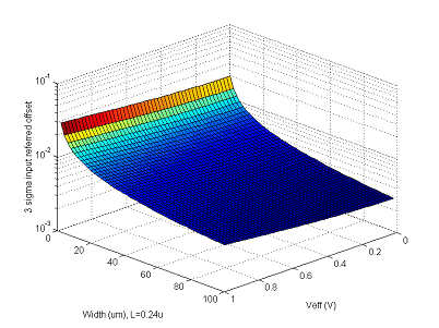
Fig. 1‑7: Offset variation with Veff and area
If 10-bit accuracy were required with a 1V signal swing,
and 1V Veff, for a successful yield of 99% (3s of the random distribution), a W of over 1968mm would be required with L=0.24mm! Clearly the larger transistor area
results in an increased parasitic gate/source/drain/bulk capacitance, requiring
increased power to operate the comparator at a fixed speed. Thus a design
tradeoff exists between speed, accuracy and power. Considering the
gain-bandwidth of a differential pair, the speed of the differential pair to a
first order [3] is given by
 (1.4) (1.4)
where square law relations are used, and drain-bulk
capacitance ignored. Noting that  , and defining accuracy [3]
as , and defining accuracy [3]
as
 (1.5) (1.5)
where b mismatch is
ignored (from Fig. 1‑7 offset is a weak function of Veff, thus
approximation is valid), the above equations are combined to yield the
following relationship [3]:
 (1.6) (1.6)
Equation (2.6) is often used as a Figure Of Merit (FOM)
for ADCs as it encapsulates three key performance metrics: speed, accuracy, and
power, as well as their associated tradeoffs with respect to the associated
technology. For example, if a designer has a fixed power and speed constraint,
higher accuracy may only be achieved by migrating to a technology that has a
smaller AVt and/or Cox. FOMs also allow for easy
comparisons between different ADC designs. (E.g.) if ADC ‘A’ reports twice the
accuracy of ADC ’B’, ‘A’ is expected to consume 4x the power of ‘B’. If ADC
‘C’ is twice as fast as ADC ‘D’, but ‘C’ consumes 3x more power than ‘D’, then
‘C’ is likely a poor design. (Assuming A, B, and C, D are in the same
technology respectively).
Another popular FOM is
 (pJ/step)
(1.7) (pJ/step)
(1.7)
where 2finput-bandwidth is the sampling rate
for Nyquist rate ADCs, fs. This figure of merit is commonly used as
the accuracy term is based on easily measured quantities, and calculates a
value that has meaningful units (i.e. energy required per conversion step).
Over the years different architectures optimal with
respect to one or more of the performance metrics mentioned in section 1.4 have
been developed. As a detailed overview of the most popular ADC architectures
would require a lengthy discussion, only a table outlining the strengths of
popular architectures is presented. The pipeline architecture however is
discussed in detail. A
more detailed discussion of alternative ADC architectures can be found in [2].
Table 1‑1: Comparison of ADC architectures
|
Architecture
|
Latency
|
Speed
|
Accuracy
|
Area
|
|
Flash
|
No
|
High
|
Low
|
High
|
|
Folding/Interpolating
|
No
|
Medium-High
|
Low-Medium
|
Medium-High
|
|
Delta-Sigma
|
Yes
|
Low
|
High
|
Medium
|
|
Successive Approximation
(SAR)
|
Yes
|
Low
|
Medium-High
|
Low
|
|
Pipeline
|
Yes
|
Medium
|
Medium-High
|
Medium
|
In a Flash ADC, the digital outputs are realized almost
immediately after the comparators are latched. The toll on the system is the
number of comparators required is at least the number of unique outputs (e.g.
1023 for 10-bit accuracy). Recalling the accuracy-power tradeoff of section 1.4,
a high accuracy implies high power consumption. Thus each of the 1023
comparators of a 10-bit flash would demand much power, making the total power
of all 1023 comparators excessively large. If however the comparison operation
is spread over several clock cycles, the number of comparators required per
clock cycle can be significantly reduced. In Fig. 1‑8, the comparison
operation is spread over two clock phases in a two-stage Flash architecture.
During the first clock phase the N/2 Most Significant Bits (MSBs) are resolved
(where N is the number of bits in the final ADC output). During the second clock
phase the resolved N/2 MSBs are removed from the input, the residue amplified
to full scale (to maintain the dynamic range, and reuse reference voltages),
and subsequently the remaining N/2 bits are resolved.

Fig. 1‑8: Two stage N-bit accurate ADC
Thus the number of comparators required in the two-stage
approach is  , which is lower than the
Flash ADC for N>2. Although speed is preserved by virtue of a queue
structure, spreading the comparison operation over time comes at the penalty of
increased conversion latency. Specifically, rather than the digital outputs
being available one clock phase after the input is sampled as in the flash
architecture, two clock phases are required for the two-step approach.
Although the first stage of the two-stage approach resolves only the first N/2
MSBs, to allow for accurate resolution of the remaining N/2 LSBs, the Digital
to Analog Converter (DAC), and subtraction blocks of the first stage must
be precise to at least N-bits. The second sample and hold however requires
only N/2+1 bits accuracy, thus has less stringent accuracy requirements.
Section 1.7 introduces the concept of digital error correction to relax the
requirements of the first stage ADC to N/2 bits. , which is lower than the
Flash ADC for N>2. Although speed is preserved by virtue of a queue
structure, spreading the comparison operation over time comes at the penalty of
increased conversion latency. Specifically, rather than the digital outputs
being available one clock phase after the input is sampled as in the flash
architecture, two clock phases are required for the two-step approach.
Although the first stage of the two-stage approach resolves only the first N/2
MSBs, to allow for accurate resolution of the remaining N/2 LSBs, the Digital
to Analog Converter (DAC), and subtraction blocks of the first stage must
be precise to at least N-bits. The second sample and hold however requires
only N/2+1 bits accuracy, thus has less stringent accuracy requirements.
Section 1.7 introduces the concept of digital error correction to relax the
requirements of the first stage ADC to N/2 bits.
The divide and conquer approach used in the two step ADC
can be extended further, such that several clock phases are used, and only a
few bits resolved per stage as illustrated in Fig. 1‑9; this generalized
approach forms the basis of a pipeline ADC [2].
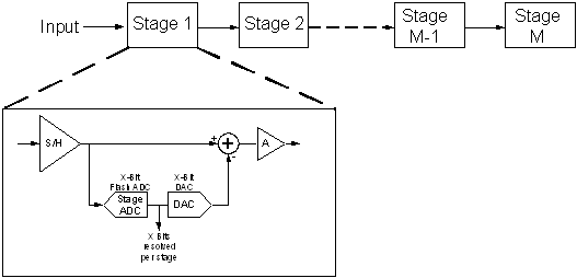
Fig. 1‑9: Pipeline ADC architecture
Although several clock phases are required for an analog
value to be digitized, a new digital output is available every clock phase.
This is due to the sequential structure shown in Fig. 1‑9, which by
virtue of sample and holds in each stage, implements a queue or pipeline
structure. Hence the throughput of the pipeline is limited by only the delay
through a single stage [2]. Pipeline ADCs are useful in configurations where
latency is not critical (e.g.) where the ADC is in an open loop signal path.
For applications where latency is critical (e.g. where the ADC is in the
critical path of a closed loop), one is restricted to using a Flash or variant
ADC.
A design tradeoff which exists for pipeline ADCs is the
choice between a larger number of bits resolved per stage (hence less latency,
but more design complexity), or a fewer number of bits resolved per stage
(hence increased latency, but simpler design). Although a proper discussion of
which trade-off is superior is beyond the scope of this discussion, it is noted
for high-speed applications with 10-bit accuracy, a longer pipeline with fewer
bits/stage is preferred [4]. A longer pipeline allows for the implementation
of fast switched-capacitor circuits with lower closed loop gains, thus smaller
feedback factors (hence faster operation [2]), and a simple digital correction
scheme to relax the precision requirements of the stage-ADCs [5].
The precision requirements of each pipeline stage decrease
through the pipeline (i.e.) the first stage must be most precise, subsequent
stages need only be as precise as the previous stage less the number of bits
resolved previously. Thus analog design complexity can be reduced along
the pipeline [6] as shown in Fig. 1‑10 (less opamp gain and bandwidth for later
stages).
Discussed in section 1.4, a relaxed precision implies a smaller area, thus
lower power consumption. Hence it is possible to significantly reduce total
power consumption by having many stages, where each subsequent stage in the
pipeline is sized smaller than the previous stage.
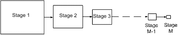
Fig. 1‑10: Pipeline stage scaling – stages are sequentially smaller
The digitization of an analog signal in a pipeline ADC is
very similar to the calculation of a quotient in long division, i.e.:

The divisor is similar to the analog input signal
(relative to full scale), the dividend the full-scale voltage (i.e. the decimal
representation of the largest 10-bit number - 1023), the quotient is the
resolved digital output word, and the remainder the quantization error. By
exploiting the long division structure of a pipeline ADC, the accuracy
requirements of the stage ADC can be relaxed. Consider the long division of
two numbers: x (divisor), and ynyn-1yn-2…y1y0
(dividend), in an arbitrary but common base b.
Both x and y are of arbitrary length, where each digit of y is explicitly shown
by the subscripts (most significant digit of y is yn, least
significant digit is y1). Thus a correct long division of y by x is
as follows:
|


----------------------------------


----------------------------------

|
* r1 is the remainder after two lines of
division
If however the divisor, x, is incorrectly divided into the
dividend, y, an incorrect remainder results, yielding every subsequent digit in
the quotient incorrect. This situation is analogous to a pipeline ADC where in
a pipeline stage a comparator in the stage Flash ADC, due to an offset,
incorrectly sets the stage DAC, leading to an incorrect value being subtracted
from the stage input. An important observation is in long division the error
is passed to the subsequent line of long division. Thus if a division error
could be identified, the error could be eliminated in the subsequent line of
long division by adjusting the quotient.
|


----------------------------------


----------------------------------

|

|
Thus if an incorrect division
is made, such that  is an incorrect digit in
the quotient, the error can be eliminated by selecting is an incorrect digit in
the quotient, the error can be eliminated by selecting  such
that r2=r1 such
that r2=r1
|
Since the correct and corrected long division approaches
yield the same remainder, the quotients in each approach are equal; despite the
fact the latter approach included a division error.
The following example numerically illustrates the concepts
discussed [7]:
|
Correct
division example

amplified residue 10
subtracted reference -
7
amplified residue 30
subtracted reference -
28
amplified residue 20
subtracted reference -
14
amplified residue 60
subtracted reference -
56
amplified residue 40
subtracted reference -
35
amplified residue 50
subtracted reference -
49
|
Error
in division, with correction example

amplified residue 10
subtracted reference -
7
amplified residue 30
subtracted reference -
28
amplified residue 20
subtracted reference -
21ßerror
amplified residue -10
subtracted reference +14
amplified residue 40
subtracted reference -
35
amplified residue 50
subtracted reference -
49
residue 1
* Note how error is
allowed to pass on to subsequent line of division, and how error is corrected
in subsequent line of division
|
Correct division quotient:

Incorrect division with corrected quotient:

From section 1.7, it is clear a finite error in long
division can be tolerated so long as the error passes to the subsequent line of
long division, and the occurrence of an error can be detected. Thus to apply
the same error correction principle to a pipeline ADC, errors caused by
comparator offsets must be passed to the subsequent pipeline stage, and a logic
implemented to recognize the occurrence of an error.
A simple pipeline topology is one that resolves two bits
per stage as shown in Fig. 1‑11, the transfer function of which is shown
in Fig. 1‑12.
|

Fig. 1‑11: Pipeline Stage detail
|
Fig. 1‑12: Stage transfer function
|
The stage gain is 4x to maximize the dynamic range of the
subsequent stage, and to allow for reuse of the reference voltages. An error
in the stage ADC threshold (due to an offset) alters the transfer function as
shown in Fig. 1‑13.
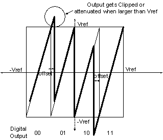
Fig. 1‑13: Over-range error with pipeline stage
Thus threshold errors lead to stage outputs that exceed
the full-scale input to the subsequent stage. As stage inputs that exceed full
scale are attenuated or clipped, offset induced errors do not pass to the
subsequent stage unaltered, and thus cannot be completely eliminated as
described in section 1.7.2. If however the stage gain is reduced to 2x as
shown in Fig. 1‑14., the error is fully passed on to the subsequent
stage, so long as the offset error does not exceed Vref/4, as shown in Fig. 1‑15.
|
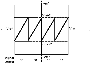
Fig. 1‑14: Reduced gain stage transfer function
|
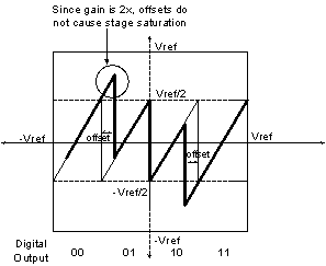
Fig. 1‑15: Impact of errors on stage transfer function
|
Hence if the subsequent stage detects an over-range error,
the error may be digitally eliminated by adding or subtracting a bit from the
digital output (depending on whether the error was an over or under range
error). Non-trivial digital subtraction is avoided by altering the transfer
function of Fig. 1‑14 by adding a Vref/4 offset [4] as shown in Fig. 1‑16:
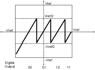
Fig. 1‑16: Vref/4 offset to eliminate digital subtraction
For error correction, each stage is required to only
determine if an over/under range error has occurred, thus the comparator at
¾Vref can be eliminated, yielding the final transfer function shown in Fig. 1‑17

Fig. 1‑17: 1.5bit/stage transfer function
With three unique digital outputs, the final transfer
function is referred to as a 1.5 bit/stage architecture.
10-bits can be resolved using 1.5 bits/stage with eight
such stages, followed by a 2-bit flash stage to resolve the final two bits
(error correction cannot be used on the last stage since there is no subsequent
stage to correct the error – note the 2-bit flash has thresholds at –Vref/2, 0,
+Vref/2). The final 10-bit output code can be realized by digitally combining
the outputs from each stage as described in [4]. A 1.5-bit/stage 10-bit
pipeline ADC was the architecture used in the ADC of this dissertation. Fig. 1‑18
illustrates the configuration of pipeline stages to yield a 10-bit output.

Fig. 1‑18: 10-bit pipeline ADC using 1.5 bits/stage
This chapter discussed the fundamental differences between
analog and digital signals, where the noise resilience of digital signaling was
shown to be superior over analog signaling. Digital signal recovery in
non-ideal channels was shown to require digital signal processing, where noise
sources were shown to necessitate ADCs in the signal path. A brief review of
Flash ADCs was given where various ADC tradeoffs between speed, power, and
accuracy motivated the use of alternative ADC topologies. The pipeline ADC was
detailed at a system level, including digital error correction, for a 1.5
bits/stage pipeline ADC.
[1]
Lathi, B.P. Modern Digital and Analog Commuincation Systems. Oxford University Press, New York, 1998
[2]
Johns, David and Martin, Ken. Analog Integrated Circuit Design.
John Wiley & Sons, Inc: New York, 1997.
[3]
Uyttenhove et al, “Speed-Power-Accuracy Tradeoff in High-Speed
CMOS ADCs”, IEEE transactions on Circuits and Systems –II: Analog and
Digital Signal Processing, vol 49, April 2002, pp. 280-287
[4]
G. Chien, “High-Speed, Lower-Power, Low-Voltage Pipelined
Analog-to-Digital Converter”, Masters of Science thesis, University of California Berkeley, 1996
[5]
S. Lewis et al, “A Pipelined 5-Msample/s 9-bit Analog-to-Digital
Converter”, IEEE Journal of Solid-State Circuits, vol SC-22, December
1987, pp. 954-961
[6]
P.T.F. Kwok et al, “Power Optimization for Pipeline Analog-to-Digital
Converters”, IEEE Transactions on Circuits and Systems--II: Analog and
Digital Signal Processing, vol 36, May 1999, pp. 549-553
[7]
D. Cline, “Noise, Speed, and Power Trade-offs in Pipelined Analog to
Digital Converters”, Doctor of Philosophy in Engineering thesis, University of California Berkeley, 1995
|
